


Your path starts here
Oregon State University was founded more than 150 years ago as a land grant institution, building on the idea that everybody deserves an extraordinary education that’s attainable and accessible. Here you can determine your purpose, shape your identity and values and become who you want to be.
Our Locations
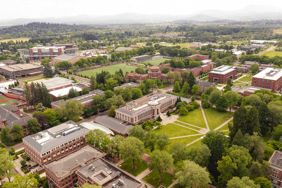
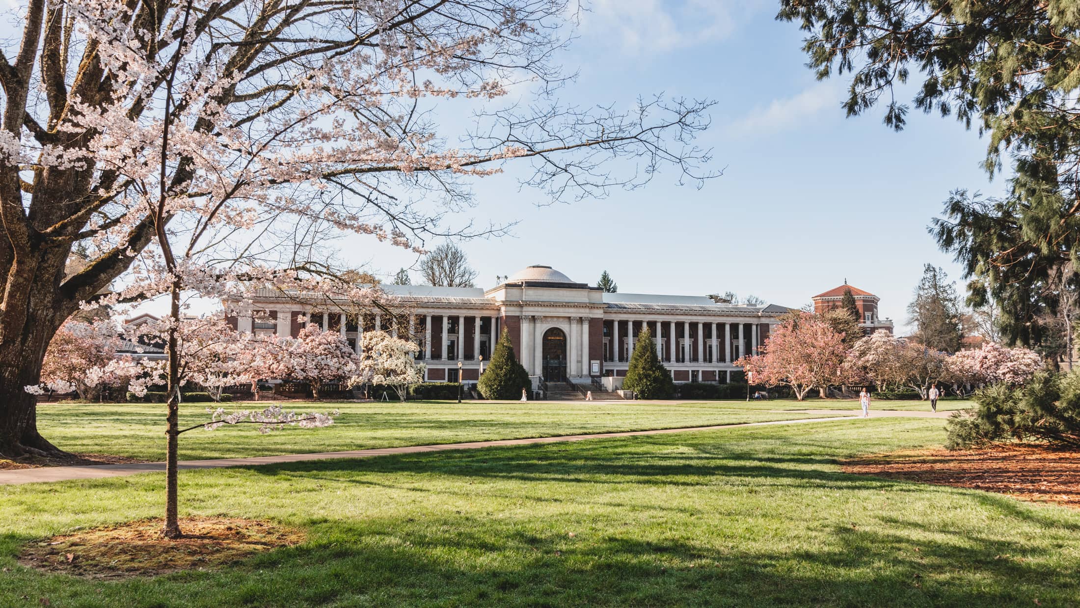
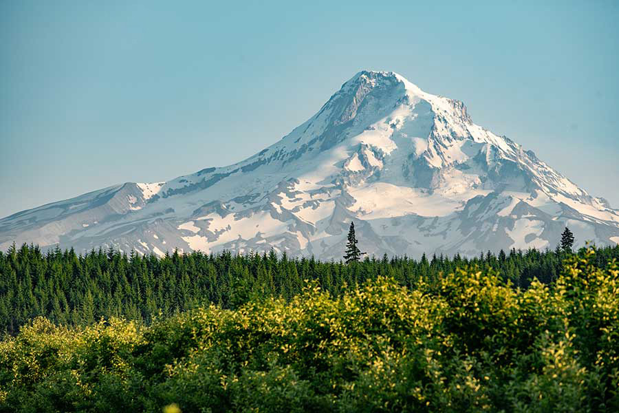
Oregon State’s beautiful, historic and state-of-the-art campus is located in one of America’s best college towns. Nestled in the heart of the Willamette Valley, Corvallis offers miles of mountain biking and hiking trails, a river perfect for boating or kayaking and an eclectic downtown featuring local cuisine, popular events and performances.
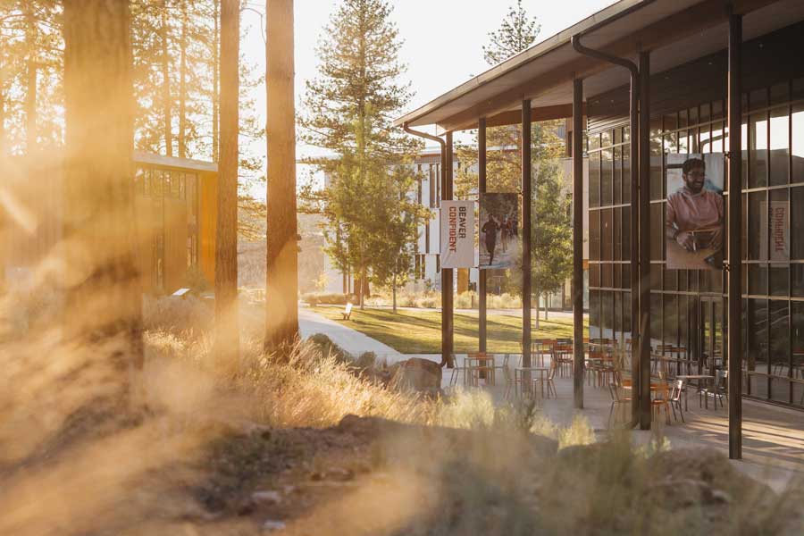
Oregon State’s Bend campus, located in the stunning high desert of Central Oregon, offers more than 20 majors, small classes and a vast natural laboratory. Nearby, endless outdoor recreation options await — including skiing, snowshoeing, rock climbing, paddle boarding and more.
Oregon State Ecampus blends 21st century innovation with 150+ years of institutional excellence to give people everywhere access to a life-changing education online. Everything we do is designed to help Oregon State students:
- Make an impact in their communities and beyond
- Feel supported along every step of their journey
- Build connections with OSU’s world-class faculty
- Enter the workforce with the skills they need to succeed
With operations in all 36 counties and the Confederated Tribes of Warm Springs, Oregon State University is a trusted partner serving Oregonians statewide. The OSU Extension Service delivers research-based knowledge and education that strengthen communities and economies, sustain natural resources and promote healthy people and families. The 11 Agricultural Experiment Stations at 14 locations address critical issues across landscapes, oceans and food systems. The Forest Research Laboratory manages 10 research forests and develops innovative approaches for managing forest resources and ecosystems.
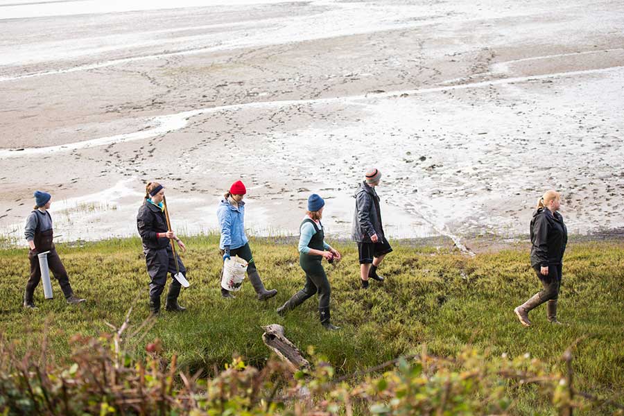
At Oregon State’s coastal research center in Newport, you can dip your toes in the Pacific Ocean — and pursue hands-on, experiential learning through classes, research and internships aimed at developing solutions to pressing environmental issues.
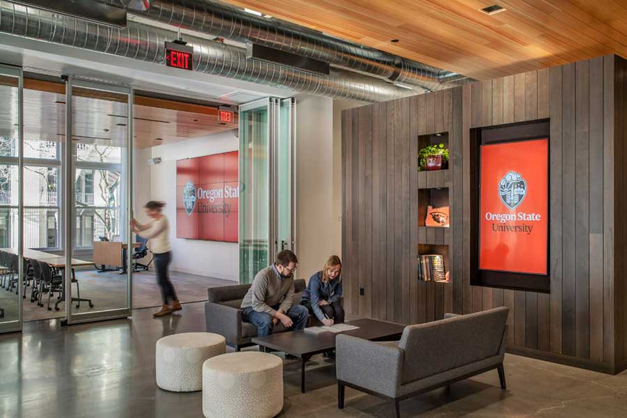
The OSU Portland Center is a premier event, meeting and conference venue for showcasing Oregon State programs, initiatives, research and exhibitions. OSU also offers a hybrid MBA and pharmacy programs, professional development courses and a variety of Extension programs in Portland.
Oregon's best public research university
With nearly 200 degree programs Oregon State has a path to the career and future you always wanted.
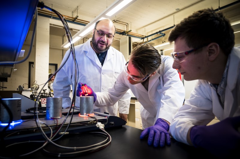
As Oregon’s largest university, we draw people from all 50 states and more than 100 countries to a welcoming community that supports success, well-being and belonging for all. We are constantly learning, innovating and applying new skills to make the world better. You can too.
Discover the people and stories of Oregon State
 Video file
 Video file
 Video file
 Video file